Si/III-V nanowires
Context
Building reliable interfaces of Si and III-V compound semiconductors may reduce fabrication costs of III-V based devices. Importantly, such III-V/Si platform provides increased possibilities in terms of materials design and novel physical properties. A stringent example is the integration of a III-V light emitter in Si.Combining Si and III-V's has been a challenge for decades because of their dissimilar properties: antiphase boundaries, dislocations, interdiffusion appear at the interfaces.
One solution is to use vapour liquid solid (VLS) grown nanowires. Thanks to their small cross-section, their reduced growth temperature and a layer by layer growth mechanism, it is possible in theory to grow defect free Si/III-V interfaces.
My postdoc project @ TU Delft
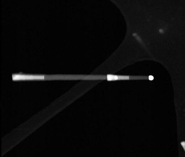
I took advantage of the VLS mechanism and the small cross section of nanowires to grow axial heterostructures. In those structures I combined Si and III-V semiconductors epitaxially to create a Si nanowire with an embedded light emitter.Growth of straight nanowires embedding segments of different materials was challenging. By a precise control of the growth parameters, arrays of Si-GaP-GaAs axial heterostructures were developed. The structures showed long life time of the excitons emitted by the GaAs segment.
I demonstrated technically that combining III-V and Si within a nanowire is possible and that it doesn’t affect neither the crystalline integrity of the materials or the optical properties of the III-V compounds.