Since 2010 I work at the Neel Institute in Grenoble.
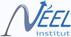
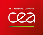
I am interested in the structure properties relation of semiconducting nanowires (NWs) using transmission electron microscopy (TEM), optical spectroscopy and electron transport. The goal of my research is to develop methods to combine various characterization methods (optical and electrical) with transmission electron microscopy characterization on the same unique nanowire, and find what structural or electrical properties at the sub-nm scale determine the macroscopically measured optical and electrical properties of the nano-structure. For electrical and electro-optical characterization contacts have to be applied to the nanowire, that can also be used to bias the nanowire device in-situ in the transmission electron microscope. Observing the reaction of a device to an electrical signal with nm scale resolution is a very exiting opportunity to learn more on the device characteristics/reactions, and will allow ultimately to correlate the presence of a single impurity atom observed in TEM with electrical spectroscopy of this same single atom in a single dopant device.