Research
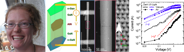
I am interested in the structure properties relation of semiconducting nanowires (NWs) using transmission electron microscopy (TEM), optical spectroscopy and electron transport. The goal of my research is to develop methods to combine various characterization methods (optical and electrical) with transmission electron microscopy characterization on the same unique nanowire, and find what structural or electrical properties at the sub-nm scale determine the macroscopically measured optical and electrical properties of the nano-structure. For electrical and electro-optical characterization contacts have to be applied to the nanowire, that can also be used to bias the nanowire device in-situ in the transmission electron microscope. Observing the reaction of a device to an electrical signal with nm scale resolution is a very exiting opportunity to learn more on the device characteristics/reactions, and will allow ultimately to correlate the presence of a single impurity atom observed in TEM with electrical spectroscopy of this same single atom in a single dopant device.
To realize these type of NW devices I fabricate nitride membranes at the Nanofab cleanroom in Neel, that are compatible with TEM and cleanroom fabrication procedures such as optical and electron beam lithography.
My research can be divided in two parts. (i) TEM characterization of semiconducting NWs to observe quantum dot insertions and other NW qualities such as cristallinity, size, strain etc. Furthermore (ii) I develop electrical in-situ experiments, working both on propagation of metals in the NW to improve the contact quality and control the size of the semiconducting region between the contacts with nm precision. Again with the idea to correlate the structural properties of the object with the electrical properties. Furthermore I use off-axis electron holography in combination with in-situ biasing with the aim to quantitatively measure doping concentration, surface charges and internal polarization fields in NWs. I have obtained promising first results looking at the depletion width at a Schotkey contact on a ZnO NW.